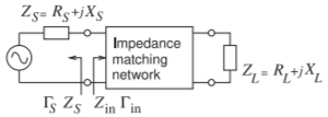
Matching networks are constructed using lossless elements such as lumped capacitors, lumped inductors and transmission lines and so have, ideally, no loss and introduce no additional noise. This section discusses matching objectives and the types of matching networks. Figure \(\PageIndex\): A source with Thevenin equivalent impedance \(Z_\) and load with impedance \(Z_\) interfaced by a matching network presenting an impedance \(Z_>\) to the source.
| Reflection-less match | Maximum power transfer |
|---|---|
| \(Z_>=Z_\) | \(\beginZ_>&=Z_^\\ \Gamma_>&=\Gamma_^\end\nonumber\) |
Table \(\PageIndex<1>\): Matching conditions with reference to Figure \(\PageIndex<1>\). \(\Gamma_>,\: \Gamma_\), must be with respect to a real \(Z_>\).
With RF circuits the aim of matching is to achieve maximum power transfer. With reference to Figure \(\PageIndex<1>\) the condition for maximum power transfer is \(Z_> = Z_^\) (see Section 2.6.2 of [1]). An alternative matching objective, used most commonly with digital circuits, is a reflection-less match. The reflection-less match and the maximum power transfer match are only equivalent if \(Z_\) and \(Z_\) are real. Nearly always in RF design the matching objective is maximum power transfer, and this is assumed unless the reflection-less match is specifically indicated. The maximum power transfer matching condition can also be specified in terms of reflection coefficients with respect to an real reference impedance \(Z_>\). (In the definition of reflection coefficient \(Z_>\) can be complex, but many of the manipulations in this book only apply when \(Z_>\) is real and this should be assumed unless it is specifically stated that it can be complex.) The condition for maximum power transfer is \(Z_> = Z_^\) which is equivalent to \(\Gamma_> = \Gamma_^\). The proof is as follows: \[\label\Gamma_>=\left(\frac
This chapter concentrates on matching network design. One emphasis here is on the development of design equations and synthesis of desired results. The second emphasis is on graphical techniques for matching network design based on using A Smith chart. This is particularly power as it enables
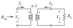
Figure \(\PageIndex\): A transformer as a matching network. Port \(\mathsf\) is on the left or primary side and Port \(\mathsf\) is on the right or secondary side.
typologies to traded-off. An alternative design approach used by some designers is to choose a circuit topology and then use a circuit optimizer to arrive at circuit values that yield the desired characteristics. This is sometimes a satisfactory design technique, but is not a good solution for new designs as it does not provide insight and does not help in choosing new topologies.
There are many design choices in the type of matching network to be developed but the common guidelines are to minimize losses and to keep the matching network compact. These objectives are not always compatible. Matching network design in this chapter is based on perfect matching at one frequency and design decisions are made to maximize, or otherwise manipulate, the bandwidth of the match. True broadband matching network design is more like filter design.
6.2: Matching Networks is shared under a CC BY-NC license and was authored, remixed, and/or curated by LibreTexts.